This article discusses in detail the photovoltaic (PV) module manufacturing processes, performance testing, quality criteria and production audits of Tier-1 PV module manufacturers in the solar energy sector. PV module production requires a rigorous process to ensure high quality standards and performance. The production stages start from raw material selection and preparation, through cell production, module building and module assembly. At each stage, quality control and performance tests are regularly performed. Performance tests are critical to assess the durability, efficiency and long-term performance of PV modules. The ability of PV modules to efficiently convert sunlight into electricity, their durability and longevity form the basis of quality criteria. These manufacturers generally adhere to industry best practices and high quality standards. Production audits are vital to ensure quality and compliance. These inspections monitor quality and ensure compliance at every step, starting from the selection of raw materials to the assembly stage. Continuous developments in the solar industry require continuous improvement of PV module manufacturing processes and quality standards. The combination of these elements contributes significantly to the development of reliable, efficient and sustainable PV module systems.
What is a Photovoltaic Cell?
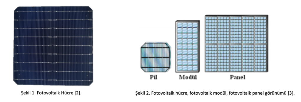
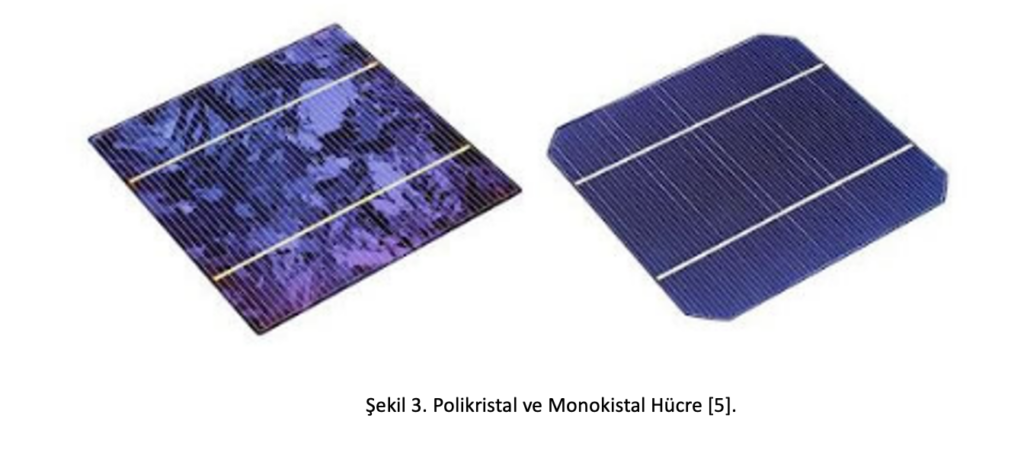
The technology that converts solar energy into electric current is called photovoltaics (PV). Photovoltaic technology, which converts solar energy into usable power, generates electricity from light. Semiconductor materials that convert sunlight directly into electrical energy are called photovoltaic cells. Photons falling on the photovoltaic cell are converted into electrical energy. When solar radiation falls on a semiconductor material, the energy of the radiation moves the atoms in the outermost orbit of the material atoms. This phenomenon is called photoelectricity. With the movement of loose atoms, electric current is generated in conductors. Electrons do work by releasing the amount of energy they carry on the obstacles they encounter. Photovoltaic cells produced with semiconductor technology are based on silicon. Photovoltaic cells are connected in series and parallel to each other and mounted on a surface. This system prepared to increase the power output is called a photovoltaic module. Figure 1 shows a photovoltaic cell, Figure 2 shows a photovoltaic module and photovoltaic panel [1].
Monocrystalline and Polycrystalline Cell
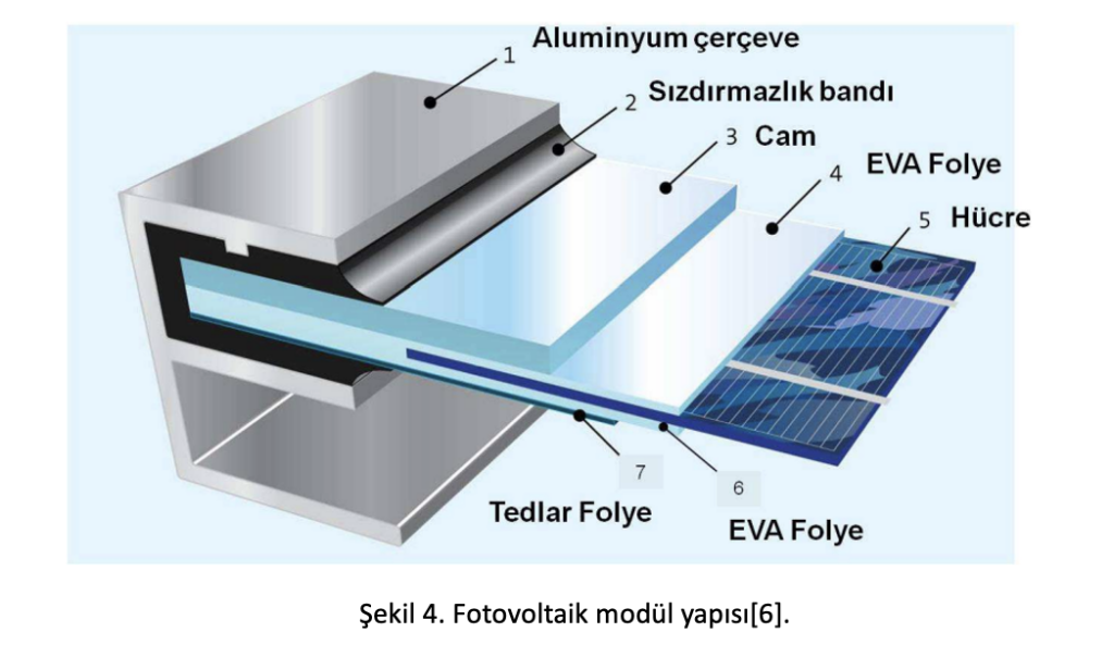
This type of photovoltaic cell uses high purity silicon crystals as raw material. There are two main types as monocrystalline and polycrystalline photovoltaic cells.
Their efficiency is higher and their lifetime is longer than cells produced by other methods.
The crystal structures of monocrystalline photovoltaic cells are regular and therefore difficult to produce and costly.
In polycrystalline photovoltaic cells, very small amounts of defects in the crystal structure cause some decrease in the efficiency of such cells. However, the ease of production and low cost compared to monocrystalline photovoltaic cells cause an increase in the tendency towards these types of cells in designs[4].
How is a Photovoltaic Module Formed?
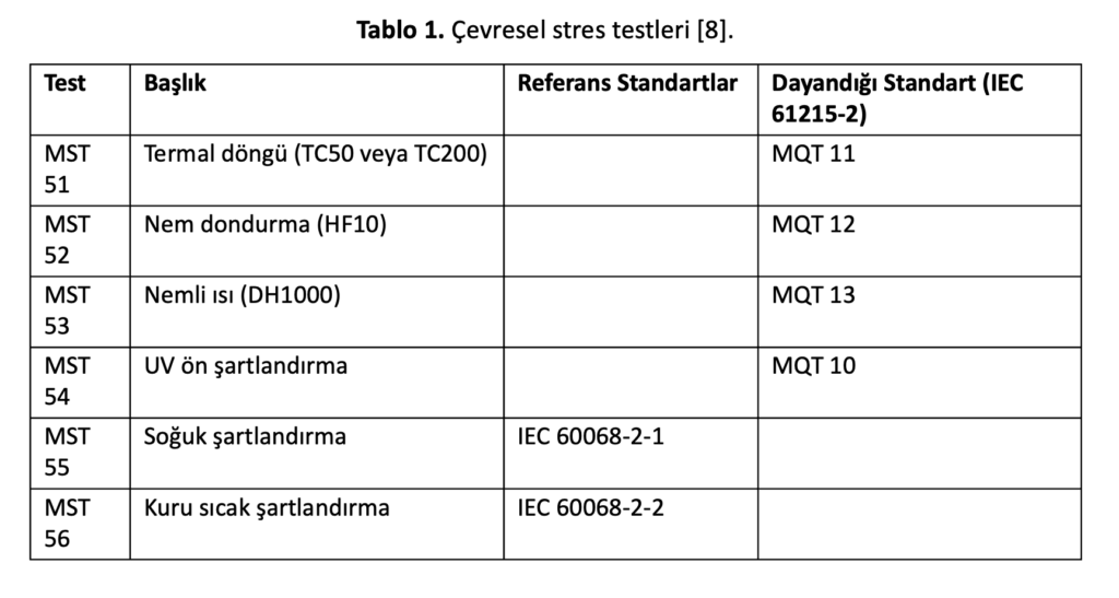
Photovoltaic modules are formed by connecting monocrystalline or polycrystalline cells in series or parallel to achieve the desired current, voltage and power values. These cells are soldered with the help of robots. After soldering, the cells are placed on a protective and highly absorbent material called ethylene-vinyl-acetate (EVA). The EVA is laid over tempered glass and protects the cells from external factors. Photovoltaic cells have EVA on both the front and back surfaces. On the back, a material called TEDLAR is used to protect the solar panel against UV rays, high temperature and humidity. The cells protected by EVA and TEDLAR are processed in special laminators under high temperature and pressure to form a single whole. Then, the junction box containing By-Pass diodes, which minimize shadowing effects, is inserted into the module. As a result of all these processes, the photovoltaic module becomes a power generator[1].
Photovoltaic Module Production Stages
TS EN IEC 61215 Terrestrial Photovoltaic (PV) modules – Design qualification and type approval
The IEC 61215 standard sets out IEC requirements for the design qualification and type approval of terrestrial photovoltaic (PV) modules suitable for long-term operation in general outdoor climates. This standard is intended to apply to all terrestrial flat plate module materials, such as crystalline silicon module types and thin film modules[7].
TS EN 61730 Photovoltaic (PV) module safety feature
IEC 61730 lists the tests that a PV module must fulfill for safety qualification. IEC 61730-2 and IEC 61730-1 are applied together for safety qualification[8].
The test sequence specified in this standard may not test all safety aspects that may be encountered in all possible applications of PV modules. Some issues, such as the electric shock hazard from a broken PV module in a high-voltage system, must be addressed through system design, location, access restrictions and maintenance procedures[8].
PV panel factories realize several combinations of all raw materials to be used in panel production, together with alternative brands. These combinations, including all materials and special components, are included in the Constructional Data Form (CDF). Panels are produced according to the CDF and many tests such as thermal cycle test, moisture freezing test, humid heat test, mechanical loading test are applied to these panels as required by IEC 61215/IEC61730 standards. Solar panels are entitled to receive a certificate if they successfully pass the tests according to IEC 61215 and IEC 61730 standards. After this stage, the panels have an approved CDF and IEC 61215/IEC 61730 certificates in addition to the CDF. The factory produces the panels according to the material list called BOM List and this BOM List must include the materials included in the CDF.
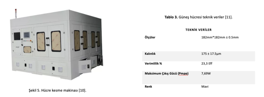
Cell Test
Solar cell testing is applied as the first process of solar panel production. During testing, the electrical performance of the cell is tested under a solar simulation. In addition, as a quality test, surface quality, undesirable negative effects such as breaks and cracks are checked [9]. Figure 5 shows the cell cutting machine.
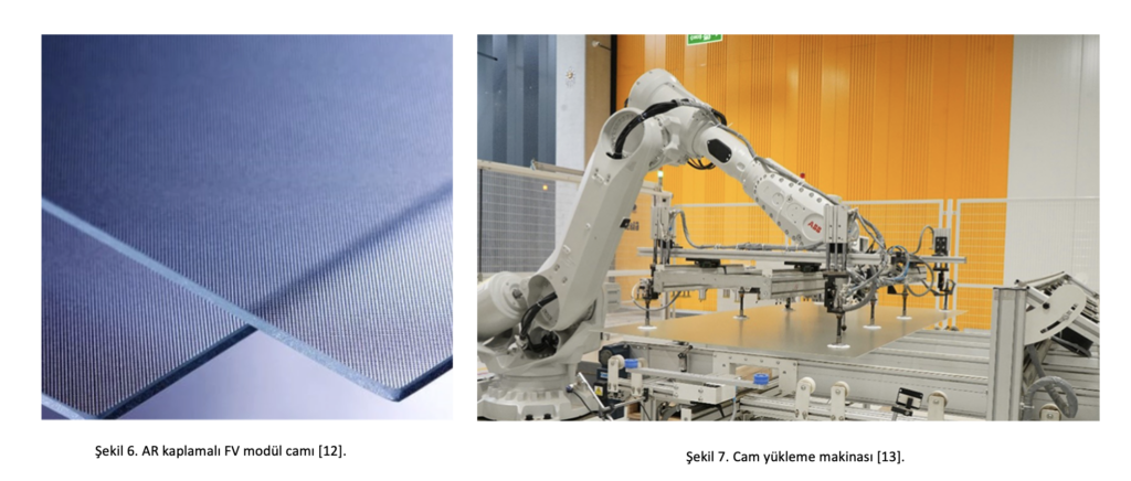
Glass Loading
The glass used in solar panel production is flat or frosted tempered glass with a low iron oxide content. The low iron oxide content increases the light transmittance of the glass. In the production line, the glass is loaded precisely by automatic robot arms. The high precision of the robot arms minimizes the risk of glass breakage and cracking during loading. After the glasses are loaded, they undergo surface control and cleaning processes. At this stage, cracks and deformations on the surface are detected [9]. Figure 6 shows the PV module glass and Figure 7 shows the glass loading machine of a factory producing PV modules.
Foil Laying Line
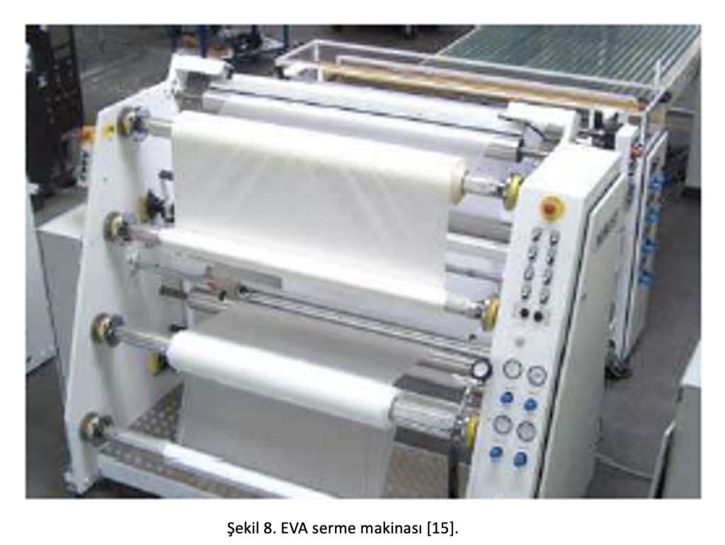
EVA (ethylene vinyl acetate) solar film is used in solar panel production systems to make electricity generation more efficient and to protect the cells against impacts. In this production line, EVA foils are combined between the glass and the cells[9]. Figure 8 shows the EVA laying machine.
EVA is a special layer that lies between the glass and the cells, as well as between the cells and the backsheet. Applied on both sides, the EVA is melted by hot lamination and completely wraps the solar cells. This process increases the durability of the panel and prevents elements such as water and micro-dust from leaking in. It also protects the solar cells by absorbing impacts and vibrations[14].
Stringer and Soldering Line
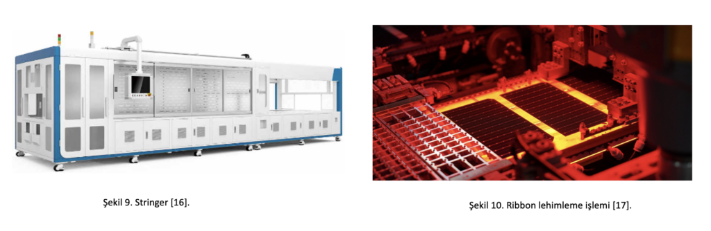
Once the microcracks and deformations on the solar cells are detected, the cells are carefully aligned on the production line. Stringer machines perform the soldering process using infrared or laser after spraying solder paste on the cells[9]. Figure 9 shows the stringer machine. In the stringer machine, conductive wires called ribbons are soldered onto the cells. Figure 10 shows a visual of the soldering process.
Lamination Line
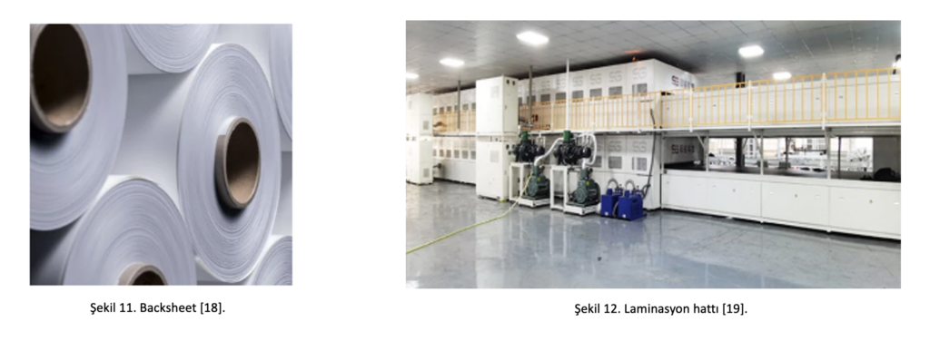
After the PV module leaves the stringer area, it is sent to the lamination line with EVA material again on the back side and either AR coated glass or a backsheet called backsheet is laid on it. Here, at high temperature and pressure, all materials are intertwined and become a whole.
Backsheets are the outer layer of solar panels and provide electrical isolation of the internal circuits from the external environment. This layer plays a critical role in protecting the panel from harsh environmental conditions. It increases the durability of solar panels throughout the panel lifetime and reduces the safety risk[14]. Figure 11 shows the backsheet used for the PV module. In the lamination line, the EVA material must melt completely at a constant time and temperature to obtain a transparent appearance and a very good grip on the cells and the entire panel [9]. Figure 12 shows the lamination line.
Press Line
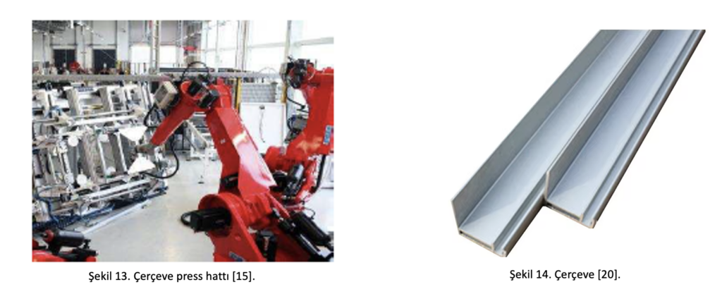
After the edge trimming and cutting of the panels and frames are done, they are sent to this line for the fitting of the frame. After the frame process is completed, the connection box is mounted to the panels [9]. Figure 13 shows the frame press line. Aluminum frames used in PV module production are important components that require attention to factors such as the appropriate design of mounting holes, set weights, coating thickness and the proportions of the elements in the content. Low iron content in aluminum frames reduces the risk of corrosion and anodized coating prevents tarnishing [14]. Figure 14 shows the frame.
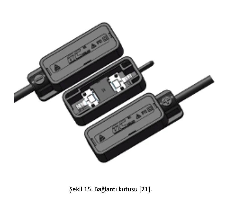
Connecting Junction Box
A junction box is attached to the modules coming out of the frame. The junction box, which connects the cells in photovoltaic solar panels in series, protects the panel electrically by transmitting the generated electricity to external lines. The diodes inside provide protection against UV rays from the sun. At the same time, this box provides access for the detection and repair of malfunctions that may occur in the panel [14]. Figure 15 shows the connection box.
The raw material checks carried out during the production audit should also be carried out for backsheet, junction box and frame. The point to be considered here is that the brand models of these products are included in the CDF. If we consider this issue especially for the junction box, there are three issues to be checked. These are bypass, cable and connector. These three elements make up the junction box. Each junction box brand can use different products for these three elements. For example, a bypass diode coded as 4045 can be used in a junction box with a rated current of 25A, while 5045 can be used for 30A. These combinations must also comply with the CDF.
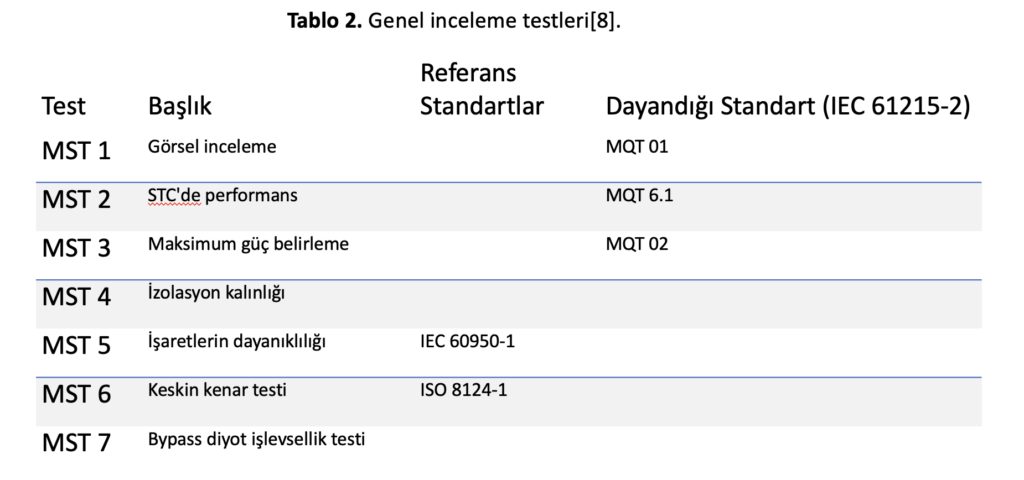
Tests Applied within the Scope of IEC 61215/IEC 61730
Visual Inspection
PV modules are inspected for the following conditions under an illumination of not less than 1000 lux.
-Cracked, warped, misaligned or torn outer surfaces
-Broken, cracked cells,
-Faulty connection points or joints,
-Cells in contact with each other or with the frame,
-Disorder of adhesive bonds,
-A continuous path between a cell and the edge of the module formed by bubbles or folds,
-Bonded surfaces of plastic materials,
-Faulty terminations exposed to live electrical parts,
-All other conditions that may affect performance [22].
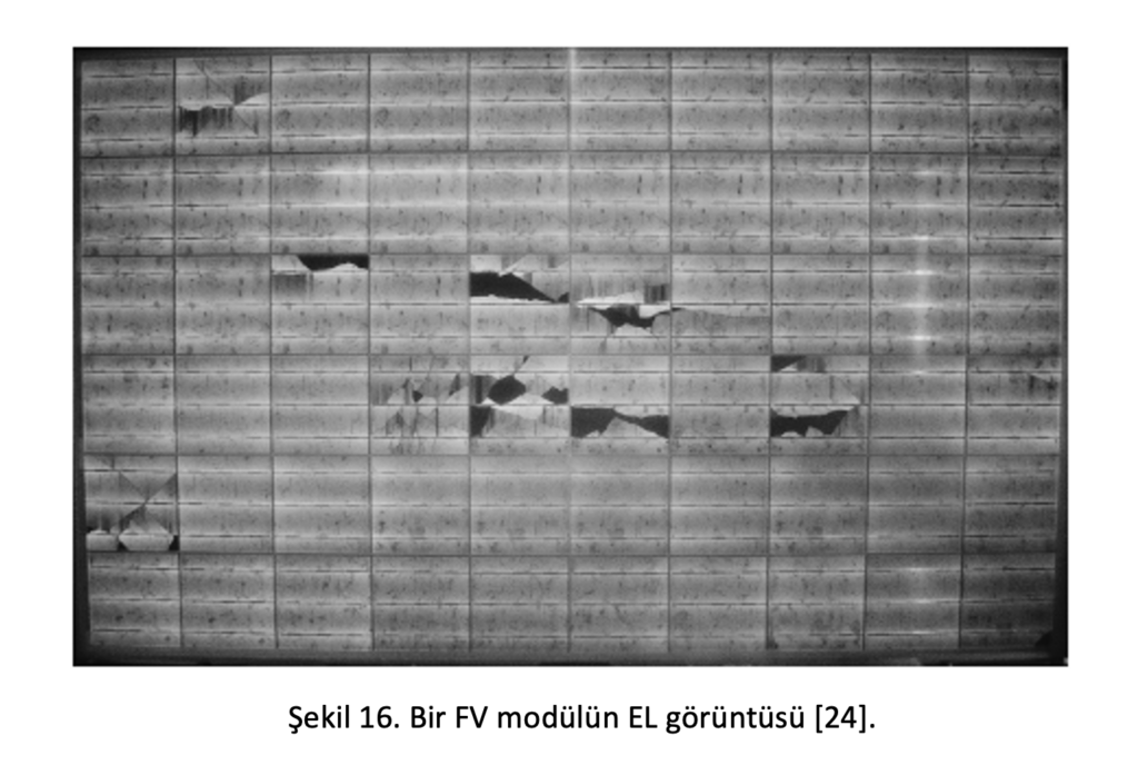
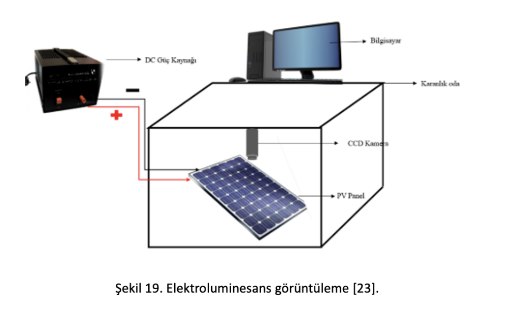
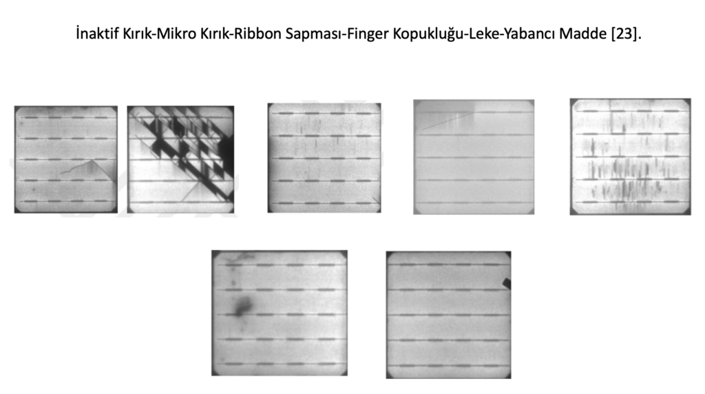
Electroluminescence (EL) images of PV modules are used to detect micro-fractures that are not visible to the eye.
Electroluminescence images are usually obtained in dimly lit environments and are usually grayscale. Defects in such images usually appear in dark regions; in particular, fractures and other defects appear as black lines or dark spots. Electroluminescence imaging is a widely used defect detection method in many manufacturers[23]. Figure 16 shows the EL image of the PV module.
Maximum Power Determination
PV module power is determined at 1000W/m² irradiance and 25°C temperature[22].
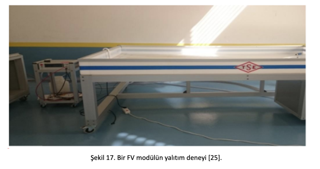
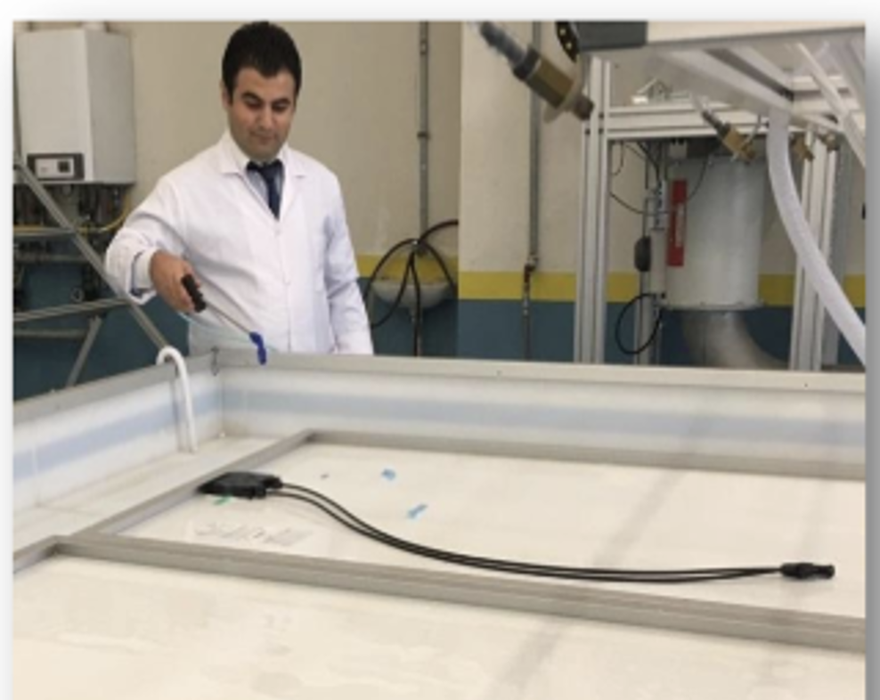
Insulation Test
This test determines whether good insulation is provided between the current-carrying parts of the module and the frame or surroundings. The insulation resistance of modules with an area of less than 0.1m2 shall not be less than 400 MΩ. For modules with more than 0.1m2, the value of the insulation resistance measured at 500 V or the maximum system voltage, whichever is greater, multiplied by the module area should not be less than 400 MΩ xm2 [22]. Figure 17 shows the TSE insulation test cabinet.
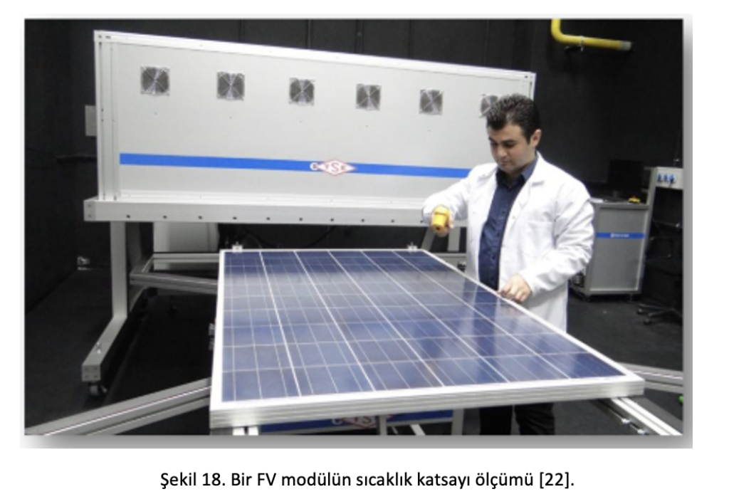
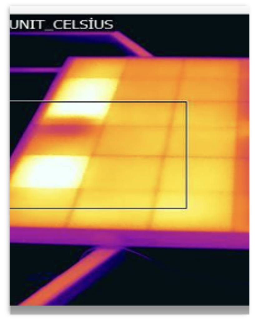
Measurement of Temperature Coefficients
Monocrystalline and polycrystalline cells with crystalline technology decrease in power as the temperature increases. The low temperature coefficient reduces energy loss when the temperature rises. When the module reaches the desired temperature,ISC, VOC and peak power are measured. The module temperature is varied in steps of about 5°C over the range of interest of at least 30°C and theISC, VOC and peak power measurements are repeated[22]. Figure 18 shows the relevant experiment.
Hot-Spot Endurance Test
The purpose of this experiment is to determine the module’s ability to withstand hot spot heating effects, for example solder melting or housing degradation can create a heating effect. This defect can also be enhanced by cracked or mismatched cells, interconnected defects, partial ghosting or blemishes. There should be no visible defects, the reduction in maximum output power should not exceed 5% of the value measured before the test and the insulation resistance should meet the initial measurements[22].
Ultraviolet PreconditioningTest (UV Preconditioning Test)
The PV module is preconditioned with ultraviolet (UV) radiation to identify materials and adhesive binders that are sensitive to UV degradation prior to thermal cycling/moisture freezing experiments. The temperature of the module is exposed to UV radiation with a wavelength band between 280 nm and 385 nm, totaling 15 kWh/m2,at 60ºC ± 5 ºC, while irradiated with UV light. [22].
Thermal Cycling Test (Thermal Cycling Test)
The ability of the PV module to withstand thermal mismatch, fatigue and other stresses caused by repeated changes in temperature is determined. 50 and 200 cycles are applied in the range from -40 °C to +85 °C. During the experiment, there should be no interruption in the current flow[22].
Humidity-Freeze Test
It determines the ability of the PV module to withstand high temperature and humidity effects following sub-zero temperatures. This is not a thermal shock test. 10 cycles are applied at +85 °C and -40 °C, 85% RH relative humidity[22].
Damp-Heat Test
It determines the ability of the PV module to withstand humidity and long-term penetration effects. 1000 hours, +85 °C, 85% RH relative humidity test is applied[22].
Wet Leakage Current Test (Wet Leakage Current Test)
This test evaluates the insulation of the PV module under wet operating conditions and verifies that moisture from rain, fog, dew or melted snow does not enter the active parts of the module circuit to cause corrosion, ground fault or safety risk[22].
-Resistance: 3,500Ω or less
-Surface Stress: 0.03 N/m or less
-Temperature: 22 ºC ± 3 ºC
For modules with an area of less than -0.1 m², the insulation resistance should not be less than 400MΩ. For modules larger than 0.1 m², the measured insulation resistance multiplied by the area of the module should not be less than 40 MΩ.m² [22].
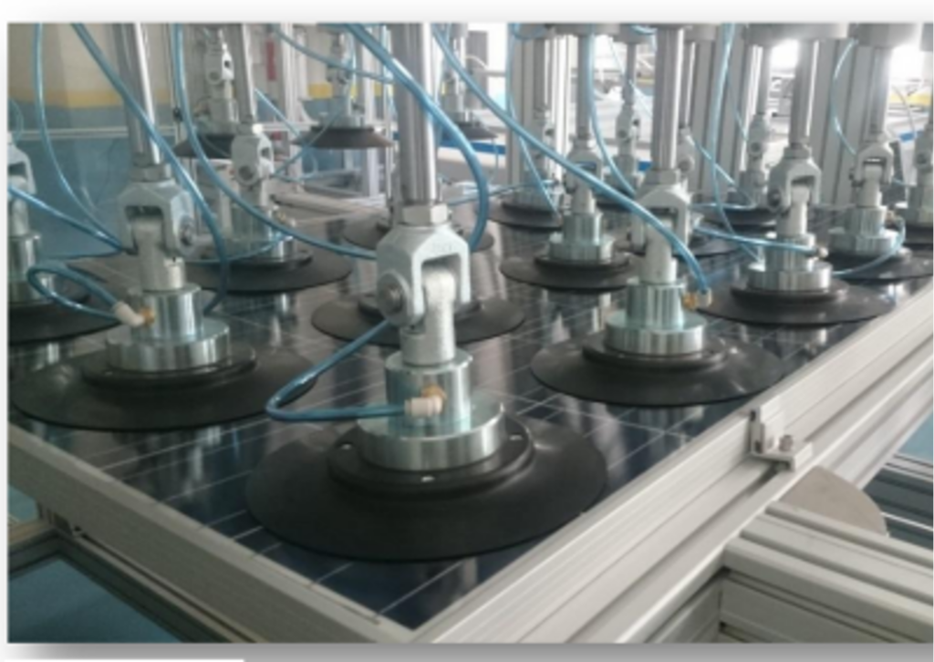
Mechanical Load Test (Mechanical Load Test)
The purpose of this experiment is to determine the resistance of a photovoltaic (PV) module to wind, land, static loads or ice loads. During the experiment, the module is fed to continuously monitor the electrical integrity of the module’s internal circuitry. A load of 2400 Pa is applied to its front and back surface for 1 hour for three cycles[22].
2400 Pa is considered as a reference for strong winds with a safety factor of 3 and a speed of 130 km/h (approximately ± 800 Pa). If the module must withstand heavy snow or ice accumulations, the force applied to the front surface of the module is increased from 2400 Pa to 5400 Pa for the last cycle. During the test no continuous open circuit fault should be detected and there should be no major visible defects. Also, the reduction in maximum output power should not exceed 5% of the value measured before the experiment[22].
Electroluminescence (EL) Imaging
Early detection of defects in photovoltaic panels is critical to ensure the efficiency, reliability and longevity of the systems. Defects can reduce panel efficiency, limit energy production and pose safety risks. These are detected through methods such as visual inspection, electrical testing and performance monitoring, and are carried out by specialized teams. Electroluminescence (EL) imaging, in particular, is widely used as a method to highlight fractures and other defects in panels. EL devices detect defects by capturing the radiation generated by DC power applied to the panels with special cameras. This process is necessary to improve the performance and lifetime of the panels during production and operation and must comply with local regulations. Detection and elimination of defects ensures optimum performance of the system, reducing operating costs and increasing environmental benefits [23].
Author:

Melisa Ekşi